Handwired Planck 40
Table of Contents
After my previous attempt to build a Corne keyboard from a premade kit bought online, I was intrigued by the electrical engineering aspect of the keyboard. I have always wanted to build a hand-wired keyboard from scratch, to learn how this thing works under the hood.
Moreover I also have a bunch of low-profile switches with a non-compatible footprint laying around, so this seems a very promising project to make use of them.
The end results is a functional, aesthetically pleasing 💭 💭 At least for me appliance, and the process is generally a very educative one
Enjoy the write up!
Cutting the acrylic plate
I found a set of DXF files online for a stacked acrylic Planck 40.
I am not much of an expert on all things CAD related. So I only opened the DXF files with FreeCAD, do some measurements, and send it to a laser cutter shop for a set of acrylic pieces
Always cut a plate at the correct thickness for the key switches to snap in. For most switches specification this is 1.5mm thick. My mistake is to cut the plate on 2mm-thick acrylic, and then the switches just keep popping out of the plate.
At the end, I need to cut 4 more sandwich layer in order for the microcontroller to fit.
Understanding the keyboard matrix
My goal when I set out to build a keyboard is to understand how it works. I wouldn’t re-explain everything here, I found this article already did that job very well. In short:
The direct GPIO method: You can connect one switch to one GPIO pin of the MCU and poll each of them.
- With n switch, you need n pins.
- You will use up all the GPIO pins for large keyboard. This method is only suitable for small board (numpad, macropad)
The better approach: keyboard matrix. We connect keys in columns and rows.
- In order to check what key is being pressed, the MCU set the each of the column to the HIGH state, then scan each row to see which of them has a HIGH state. This will give the MCU the coordinate of they key being pressed (row x, col y) 1 1 Note that this is only a simple scanning methodology. The Charlieplex method, for example, allow even more efficient use of GPIO pins: max(m, n) pins for m×n switches, at a bit of tradeoff in sensitivity:
- A diode is needed to ensure that the current only flow from the column wire, through the switch, into the row wire. Without it, a weird behavior named ghosting will happen when we press multiple keys. 2 2 Explanation here
- The number of pins needed for a m rows × n columns matrix is n + m.
Soldering the switch matrix
Switch and diodes
I follow the tips here: A modern handwiring guide - stronger, cleaner, easier | Geekhack
First we prep the diodes. I use a fine-tip tweezer to make a loop on the anode (-) leg, the leg without the black band. The guide told me to bend all the diodes when they are still in the tape so they got bent at the same location, but because I got the diodes in a zip bag I just bend them all by hand. After making an initial loop, use a plier/tweezer and pull the loop a little bit tighter. Do this for as much diodes as there are switches.
I chose some Zener diodes (1N4733). Note that for this purpose any diode will do. I like those glass diodes because it has a distinctive orange color.
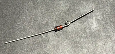
Soldering the diodes on the switches is pretty easy if you got the loop right. If you pull the loop tight enough, the diode stays in place mechanically. Then apply some solder.
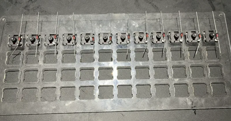
I did two rows, then I wanted to solder the wires on those rows immediately just to see how it looks like.
Soldering rows and columns
I tried sourcing a bunch of wires for this. Per the tips, I tried to find single-core insulated wires around 24-26 AWG (0.5mm ish). The best place to get this is by cutting up some old 💭 💭 I don’t have any spare around so I just buy some new one, it’s dirt cheap anyway Ethernet cables. They are also quite colorful.
The tools needed for this is a tool to cut and strip insulation. You can even make do with an X-Acto, but you should invest in a vise-grip wire stripper, something like this.

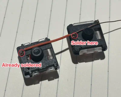
The general process that I find works best for this is as follow. The photos is a reenaction of the process, I forgot to take picture when I was doing it.
- Strip off a long piece of insulation first, exposing a long core. You need at least about 3mm × number of switches per row/column, but I cut more than that just to be sure.
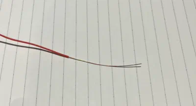
- For each adjacent pair of diodes/switch lead on the row/column, cut a piece of insulation enough to cover the wire between them. I will measure the distance between them, then minus about 1–2mm to cover for the joint. Because I’m building an all 1u ortho-linear, every pieces of insulation have the same distance. On a normal layout keyboard you will need to do precise measuring.
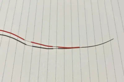
- Start soldering the wire onto the first switch/diode
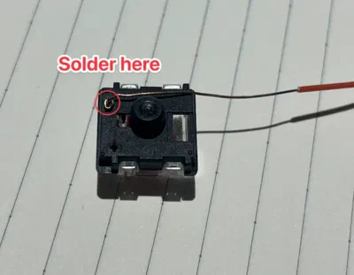
- Shift the piece of insulation next to the solder joint, then wrap a loop around the next joint and solder it.
Here are the results:
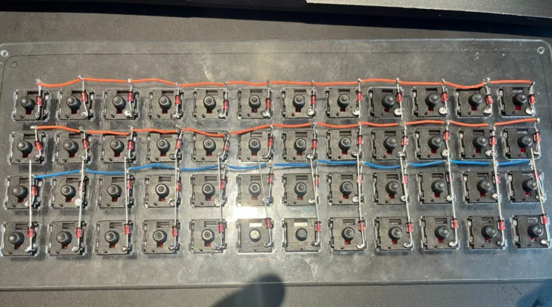
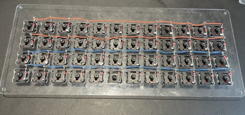
You do the same thing for the columns, on the free leg of the switch. I forgot to take picture of the column soldered. The process is largely the same.
When you grab the acrylic from the laser cutting shop, it is probably covered in a brown paper-like protective film. Don’t peel it off after you are done.
MCU socket
For the MCU, I’m using the ProMicro/SuperMini NRF52840 3 3 Being a clone, there are some manufacturing shortcoming. , which is a much cheaper Chinese clone of the nice!nano, which in turns match the footprint and pin layout of an Arduino ProMicro. However, a nice!nano will fetch me at least 5. This board pack a lot of nice feature for a keyboard.
- Seamless wired, bluetooth
- Charging circuitry included for a little Li-Po battery
I was pretty impressed with how easy it is to get this board up and running when building the corne , so I decided to use one for this build as well.
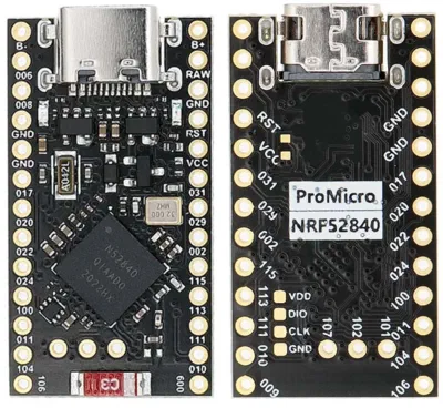
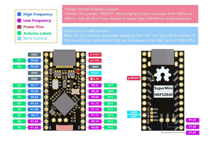
I am building a keyboard with 4×12 keys, so I will need 16 GPIO pins for the matrix scanning. Conveniently, the board have 16 standard pins at the bottom for GPIO.
First, I fashioned a board to plug the MCU on. I use a perfboard, two machined-pin socket rails and a ribbon cable. A power switch is also installed, so I can conveniently disconnect the battery.
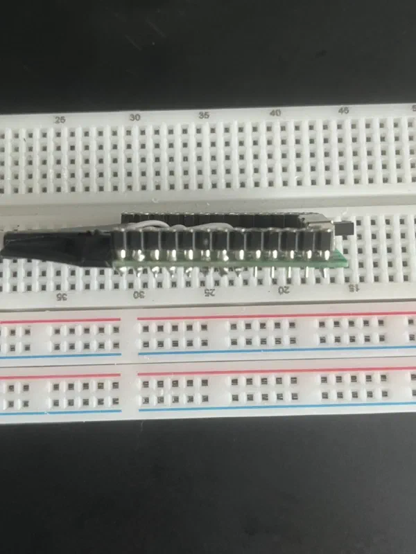
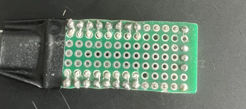
I redo the socket so the wire comes from under the board. I intend to leave the top side for a socket to install an OLED screen.
Then I soldered some pins to the ProMicro. This guide show how to install it. The result is a flush fit between the MCU board and the socket. (todo: pictures here).
I also solder up the common ground pins & a cable for plugging in a Li-Po battery
Wiring into the matrix
Next I solder the ribbon cable into the rows & columns. At this point, I decided to just solder the wires however I see fit, then I will find out which pin on the socket correspond to which row/column. For this part, put the socket/board thing in place, then split up the ribbon cable into strands and solder them to each row/column. You don’t have to be very precise, the ribbon strands can be soldered anywhere on each row/column wire. I like to slide them beneath the row/column wires to keep them neat & in place.
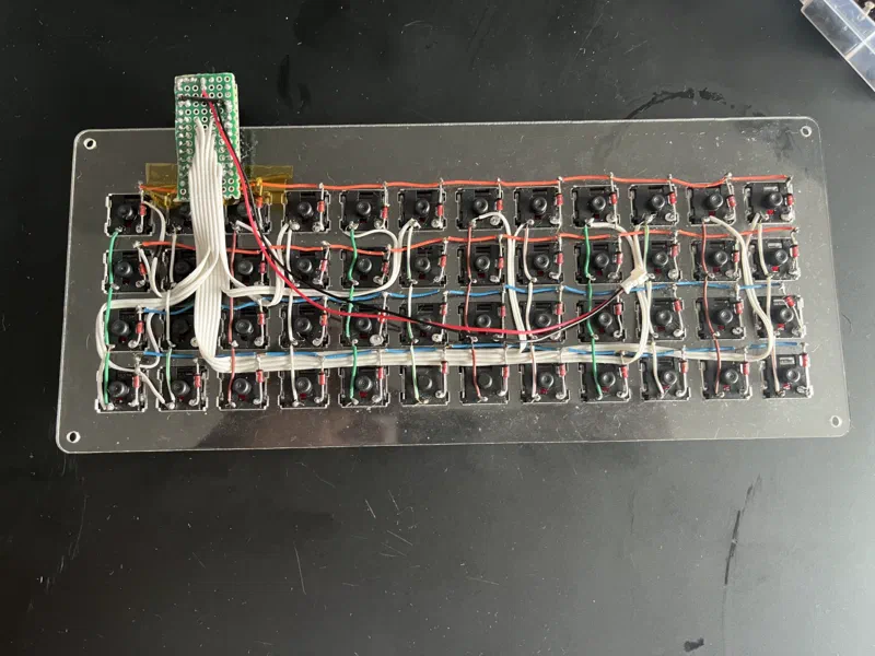
Afterward, I use a multimeter to determine which pin correspond to which row/column. I note down the row/column number -> arduino label of the corresponding pin.
The multi-meter apply a voltage to detect connectivity. I don’t know if applying voltage to the pin is safe, but I don’t wanna risk frying the board. Better safe than sorry.
Configuring ZMK
For the firmware, I’ll use ZMK. The process of defining a custom keyboard in ZMK is a little bit complex and took me a bit of reading to understand. In short, I need to do this 4 4 The full guide is in ZMK’s doc site. .
- Install the ZMK cli
uv tool install zmk - Create a
zmk-configrepository from a template - Define my keyboard physical layout & capability
- Push the code to GitHub. The ZMK project leverages Github Action to build firmware files
I am not an experience zmk user/developer. The way I structured the files might not be optimal
💭
💭
I saw some mentioning about ZMK modules which could be a better tool to organize this
, but it works for me.
Defining a new physical layout
The ZMK project define two electrical component: the shield is a large, dumb PCB where switches are installed on, and the board is the MCU. The two are configured separately. In my build, the whole hand-wired installation is the shield, and the ProMicro is the board. Because the board is already in-tree, under the nice_nano name, I will only need to define the shield definition.
I adapt the
configuration from the in-tree boardsource5x12 shield, because it is pretty similar to the Planck 40, just minus 1 row.
In the zmk-config repository, create the following files
zmk-config
├── boards
    └── shields
        └── planck40
            ├── Kconfig.defconfig
            ├── Kconfig.shield
            ├── planck40.conf
            ├── planck40.keymap
            ├── planck40.overlay
            └── planck40.zmk.yml
The content should looks like this:
Kconfig.defconfig:
if SHIELD_PLANCK40

config ZMK_KEYBOARD_NAME
    default "Planck 40"

endif # SHIELD_PLANCK40
Kconfig.shield
config SHIELD_PLANCK40
    def_bool $(shields_list_contains,planck40)
planck40.overlay
#include <dt-bindings/zmk/matrix_transform.h>

#include <layouts/common/ortho_4x12/all1u.dtsi>

/ {
    chosen {
        zmk,kscan = &kscan0;
        zmk,physical-layout = &layout_ortho_4x12_all1u;
    };


    kscan0: kscan {
				# keyscan driver
        compatible = "zmk,kscan-gpio-matrix";
        wakeup-source;

        diode-direction = "col2row";

        row-gpios
            = <&pro_micro 19 (GPIO_ACTIVE_HIGH | GPIO_PULL_DOWN)>
            , <&pro_micro 21 (GPIO_ACTIVE_HIGH | GPIO_PULL_DOWN)>
            , <&pro_micro 15 (GPIO_ACTIVE_HIGH | GPIO_PULL_DOWN)>
            , <&pro_micro 16 (GPIO_ACTIVE_HIGH | GPIO_PULL_DOWN)>
            ;

        col-gpios
            = <&pro_micro 10 GPIO_ACTIVE_HIGH>
            , <&pro_micro 14 GPIO_ACTIVE_HIGH>
            , <&pro_micro 3 GPIO_ACTIVE_HIGH>
            , <&pro_micro 5 GPIO_ACTIVE_HIGH>
            , <&pro_micro 18 GPIO_ACTIVE_HIGH>
            , <&pro_micro 20 GPIO_ACTIVE_HIGH>
            , <&pro_micro 7 GPIO_ACTIVE_HIGH>
            , <&pro_micro 9 GPIO_ACTIVE_HIGH>
            , <&pro_micro 6 GPIO_ACTIVE_HIGH>
            , <&pro_micro 8 GPIO_ACTIVE_HIGH>
            , <&pro_micro 2 GPIO_ACTIVE_HIGH>
            , <&pro_micro 4 GPIO_ACTIVE_HIGH>
            ;
    };

    matrix_transform_40_all1u: keymap_transform_0 {
				# electrical event into keyslot mapping
        compatible = "zmk,matrix-transform";
        columns = <12>;
        rows = <4>;
        map = <
            RC(0,0) RC(0,1) RC(0,2) RC(0,3) RC(0,4) RC(0,5) RC(0,6) RC(0,7) RC(0,8) RC(0,9) RC(0,10) RC(0,11)
            RC(1,0) RC(1,1) RC(1,2) RC(1,3) RC(1,4) RC(1,5) RC(1,6) RC(1,7) RC(1,8) RC(1,9) RC(1,10) RC(1,11)
            RC(2,0) RC(2,1) RC(2,2) RC(2,3) RC(2,4) RC(2,5) RC(2,6) RC(2,7) RC(2,8) RC(2,9) RC(2,10) RC(2,11)
            RC(3,0) RC(3,1) RC(3,2) RC(3,3) RC(3,4) RC(3,5) RC(3,6) RC(3,7) RC(3,8) RC(3,9) RC(3,10) RC(3,11)
            >;
    };
};

&layout_ortho_4x12_all1u {
    transform = <&matrix_transform_40_all1u>;
};
This file define how to map electrical events into keyboard event. The kscan0 node defines the GPIO labels corresponding to each row/column. The matrix_transform_40_all1u node defines how to map an matrix event to a location on the keyslot.
You need to define the row-gpios and col-gpios to match your mapping from the
Wiring into the matrix step.
planck40.keymap
#include <behaviors.dtsi>
#include <dt-bindings/zmk/bt.h>
#include <dt-bindings/zmk/keys.h>
#include <dt-bindings/zmk/outputs.h>
/ {
keymap {
compatible = "zmk,keymap";
default_layer {
display-name = "Default Layer";
bindings = <
&kp ESCAPE &kp Q &kp W &kp E &kp R &kp T &kp Y &kp U &kp I &kp O &kp P &kp BACKSPACE
&mt CAPS TAB &kp A &kp S &kp D &kp F &kp G &kp H &kp J &kp K &kp L &kp SEMI &kp SQT
&kp LSHIFT &kp Z &kp X &kp C &kp V &kp B &kp N &kp M &kp COMMA &kp DOT &kp FSLH &kp RET
&kp GLOBE &kp LCTRL &kp LALT &kp LGUI < 1 SPACE &kp SPACE &kp SPACE < 2 SPACE &kp LEFT &kp DOWN &kp UP &kp RIGHT
>;
};
raise_layer {
display-name = "Raise Layer";
bindings = <
&kp TILDE &kp EXCL &kp AT &kp HASH &kp DLLR &kp PRCNT &kp CARET &kp AMPS &kp ASTRK &kp LPAR &kp RPAR &kp DEL
&trans &kp F1 &kp F2 &kp F3 &kp F4 &kp F5 &kp F6 &kp UNDER &kp PLUS &kp LBRC &kp RBRC &kp PIPE
&trans &kp F7 &kp F8 &kp F9 &kp F10 &kp F11 &kp F12 &kp LS(NON_US_HASH) &kp LS(NON_US_BSLH) &trans &trans &trans
&trans &trans &trans &trans &trans &trans &trans &mo 3 &kp C_NEXT &kp C_VOL_DN &kp C_VOL_UP &kp C_PLAY_PAUSE
>;
};
lower_layer {
display-name = "Lower Layer";
bindings = <
&kp GRAVE &kp N1 &kp N2 &kp N3 &kp N4 &kp N5 &kp N6 &kp N7 &kp N8 &kp N9 &kp N0 &kp DEL
&kp DEL &kp F1 &kp F2 &kp F3 &kp F4 &kp F5 &kp F6 &kp MINUS &kp EQUAL &kp LBKT &kp RBKT &kp BSLH
&trans &kp F7 &kp F8 &kp F9 &kp F10 &kp F11 &kp F12 &kp NON_US_HASH &kp NON_US_BSLH &trans &trans &trans
&trans &trans &trans &trans &mo 3 &trans &trans &trans &trans &trans &trans &trans
>;
};
adjust_layer {
display-name = "Adjust Layer";
bindings = <
&kp F1 &kp F2 &kp F3 &kp F4 &kp F5 &kp F6 &kp F7 &kp F8 &kp F9 &kp F10 &kp F11 &kp F12
&trans &none &none &none &none &none &none &none &none &none &none &kp PSCRN
&trans &none &none &none &none &none &none &none &none &none &none &kp LC(DEL)
&trans &trans &trans &trans &trans &bootloader &bootloader &trans &trans &trans &trans &tog 4
>;
};
flock_layer {
display-name = "Flock Layer";
bindings = <
&kp F1 &kp F2 &kp F3 &kp F4 &kp F5 &kp F6 &kp F7 &kp F8 &kp F9 &kp F10 &kp F11 &trans
&out OUT_TOG &bt BT_SEL 0 &bt BT_SEL 1 &bt BT_SEL 2 &bt BT_SEL 3 &bt BT_SEL 4 &bt BT_PRV &bt BT_NXT &bt BT_CLR &trans &trans &trans
&trans &trans &trans &trans &trans &trans &trans &trans &trans &trans &trans &trans
&trans &trans &trans &trans &trans &trans &trans &trans &trans &trans &trans &tog 3
>;
};
};
};
This is the keymapping, from a keyslot on the physical layout into one key event. You don’t have to worry too much about this file as it is only a default template, and there is a visual editor that I’ll explore later.
planck40.zmk.yml
file_format: "1"
id: planck40
name: planck40
type: shield

# Set this to a URL that documents the keyboard.
url: https://example.com

# Add any features your keyboard supports here.
# See https://zmk.dev/docs/development/hardware-integration/hardware-metadata-files#features
features:
  - keys
  - studio # Remove this line if your keyboard will not support ZMK Studio

requires:
  - pro_micro
That’s enough for defining the new custom shield. Let’s continue with configuring the build process.
Adding Planck40 into my build
From the zmk-config repository
5
5
You can run zmk cd to navigate into it, provided that you init zmk-cli properly per the guide.
, run zmk keyboard add, choose the new planck40 shield and nice_nano_v2 controller.
Edit the build.yml file at the root:
include:
  - board: nice_nano_v2
    shield: planck40
    cmake-args: -DCONFIG_ZMK_STUDIO=y
    artifact-name: planck40_studio
  - board: nice_nano_v2
    shield: settings_reset
    artifact-name: settings_reset
When pushing this config onto GitHub, this will build a planck40_studio.uf2 and settings_reset.uf2 file. The settings reset firmware is used when you want to clean up some persisted value onboard.
Flashing the firmware
When I first buy the MCU, it is already in bootloader mode. If it isn’t, plug it into the computer, then set it to bootloader mode by shorting the pin RST & GND (they are adjacent) twice under 0.5s 💭 💭 I intended to solder a push button there for this, but I realize once I have a functioning bootloader, I can bind a key combination to go into bootloader mode. .
When in bootloader mode, the board will show up on the computer as a disk drive named NICENANO. Paste the uf2 file into the drive to flash it.
The socket is rather a flush fit, pulling it out takes a bit of care. Therefore you should first try to flash a firmware and confirm the board works before installing it. Plug the board into the computer, flash a keymap, then connect a row pin to a column pin and see if it send some keyboard event?
Editing the keymap visually
We can edit the keymap file in text, but it is really unintuitive. There is
a tool by Nick Coutsos for editing zmk keymap. In order to use it for our Planck keyboard, add a config/planck40.json into the zmk-config repo.
// config/planck40.json

{
  "id": "planck40",
  "name": "Planck 40",
  "layouts": {
    "default_transform": {
      "name": "default_transform",
      "layout": [
        { "row": 0, "col":  0, "x":     0, "y": 0 },
        { "row": 0, "col":  1, "x":     1, "y": 0 },
        { "row": 0, "col":  2, "x":     2, "y": 0 },
        { "row": 0, "col":  3, "x":     3, "y": 0 },
        { "row": 0, "col":  4, "x":     4, "y": 0 },
        { "row": 0, "col":  5, "x":     5, "y": 0 },
        { "row": 0, "col":  7, "x":     6, "y": 0 },
        { "row": 0, "col":  8, "x":     7, "y": 0 },
        { "row": 0, "col":  9, "x":     8, "y": 0 },
        { "row": 0, "col": 10, "x":     9, "y": 0 },
        { "row": 0, "col": 11, "x":    10, "y": 0 },
        { "row": 0, "col": 12, "x":    11, "y": 0 },

        { "row": 1, "col":  0, "x":     0, "y": 1 },
        { "row": 1, "col":  1, "x":     1, "y": 1 },
        { "row": 1, "col":  2, "x":     2, "y": 1 },
        { "row": 1, "col":  3, "x":     3, "y": 1 },
        { "row": 1, "col":  4, "x":     4, "y": 1 },
        { "row": 1, "col":  5, "x":     5, "y": 1 },
        { "row": 1, "col":  7, "x":     6, "y": 1 },
        { "row": 1, "col":  8, "x":     7, "y": 1 },
        { "row": 1, "col":  9, "x":     8, "y": 1 },
        { "row": 1, "col": 10, "x":     9, "y": 1 },
        { "row": 1, "col": 11, "x":    10, "y": 1 },
        { "row": 1, "col": 12, "x":    11, "y": 1 },

        { "row": 2, "col":  0, "x":     0, "y": 2 },
        { "row": 2, "col":  1, "x":     1, "y": 2 },
        { "row": 2, "col":  2, "x":     2, "y": 2 },
        { "row": 2, "col":  3, "x":     3, "y": 2 },
        { "row": 2, "col":  4, "x":     4, "y": 2 },
        { "row": 2, "col":  5, "x":     5, "y": 2 },
        { "row": 2, "col":  7, "x":     6, "y": 2 },
        { "row": 2, "col":  8, "x":     7, "y": 2 },
        { "row": 2, "col":  9, "x":     8, "y": 2 },
        { "row": 2, "col": 10, "x":     9, "y": 2 },
        { "row": 2, "col": 11, "x":    10, "y": 2 },
        { "row": 2, "col": 12, "x":    11, "y": 2 },


        { "row": 3, "col":  0, "x":     0, "y": 3 },
        { "row": 3, "col":  1, "x":     1, "y": 3 },
        { "row": 3, "col":  2, "x":     2, "y": 3 },
        { "row": 3, "col":  3, "x":     3, "y": 3 },
        { "row": 3, "col":  4, "x":     4, "y": 3 },
        { "row": 3, "col":  5, "x":     5, "y": 3 },
        { "row": 3, "col":  7, "x":     6, "y": 3 },
        { "row": 3, "col":  8, "x":     7, "y": 3 },
        { "row": 3, "col":  9, "x":     8, "y": 3 },
        { "row": 3, "col": 10, "x":     9, "y": 3 },
        { "row": 3, "col": 11, "x":    10, "y": 3 },
        { "row": 3, "col": 12, "x":    11, "y": 3 }
      ]
    }
  },
  "sensors": []
}
Open the tool, authorize it to see the zmk-config GitHub repository. You will see a visual editor of the keymap like this:
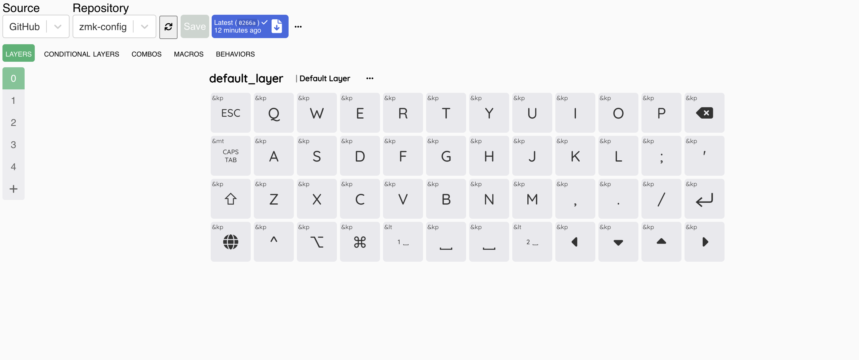
Saving the keymap will push a new commit onto the GitHub repository, then trigger the GitHub action build automatically. You can download the UF2 file afterward, then flash it onto the board.
Final assembly
After putting the board into the socket and testing that it works, I connected the battery & assembled the acrylic sandwich case. I add a bit of Kapton tape to hold the MCU socket in place.
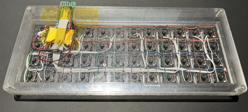
Save you some times to take it apart and clean it then assemble it again. Or if you follow my previous tip and keep the protective film on, this tip isn’t needed.
Slap some keycap on and the whole thing is finished.
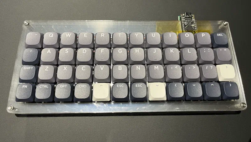
If you make a mistake like me and cut a 2mm plate, be really careful when pulling a keycap. There’s very little force holding the switch in place. Use some tweezer to hold the switch in place before using a keycap puller. Pull it too hard, you risk damaging the row/column wires or the switch itself, and it’s really messy to fix a handwired keyboard.
Final words
Personally this project is really one of the most satisfying thing I have done in a while. Learn how such a simple appliance like a keyboard work taught me a bit about electrical engineering and embedded programming. I attempted to build this by myself, researching only material online without the help of LLMs. The rather arduous process engaged my brain and overall makes the whole experience much more rewarding.
References
- Handwired Keyboard Build Log - Part 2 - Masterzen’s Blog
- Building a Handwired Keyboard : 9 Steps - Instructables